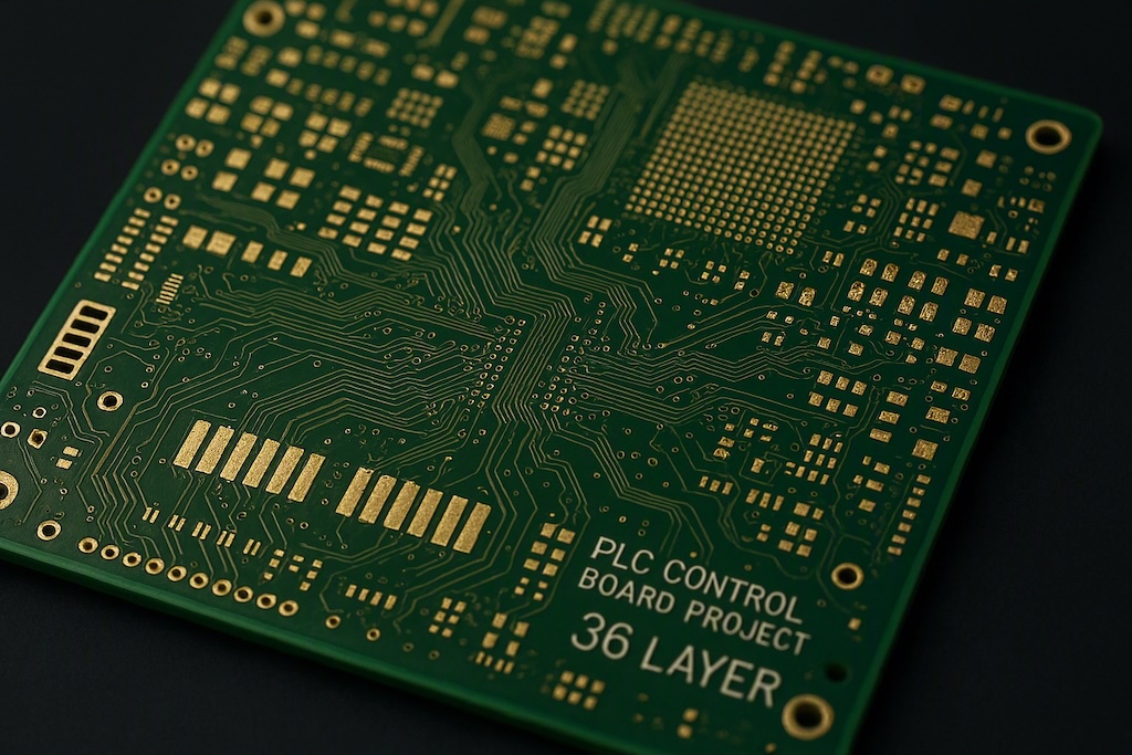
36-Layer Industrial Control PCB — Project Case Study

Kejie PCB is a 36 layer PCB manufacturer with proven capability for high-layer-count industrial applications — this case study covers a PLC controller board produced for an industrial automation client in Argentina.

Project Overview box

ApplicationPLC Controller — Industrial Automation
Layer Count36 layers
MaterialIsola High-Performance Laminate
Surface FinishENIG (Electroless Nickel Immersion Gold)
Copper Weight2oz
Board Dimensions220mm x 150mm
TestingAOI + Impedance Testing
Customer LocationArgentina
Production TypeCustom Production Run
36 layer industrial control PCB ENIG finish Isola laminate

Project Background

This project was commissioned by an industrial automation company in Argentina requiring a high-layer-count PCB for a PLC (Programmable Logic Controller) application. PLC controllers demand exceptional signal integrity across multiple power and signal planes, precise impedance control, and reliable thermal management under continuous operating conditions.

At 36 layers, this board sits at the upper end of standard multilayer PCB complexity — requiring sequential lamination cycles, precise layer registration and controlled impedance routing across the full stack-up.

Engineering Challenges

Thermal Management
With 2oz copper weight across 36 layers, managing heat distribution through the board stack was the primary engineering challenge. Copper planes were strategically arranged to act as thermal spreaders, distributing heat away from high-power components in the PLC control circuitry. Our CAM engineers reviewed the stack-up specifically for thermal via placement and copper balance before production started.

Layer Registration
Producing a 36-layer board with consistent layer-to-layer registration across the full 220mm x 150mm format requires precise press control and multiple sequential lamination cycles. Any misregistration at this layer count compounds through the stack and affects via reliability. Our manufacturing team applied tight press cycle parameters to maintain registration tolerance throughout.

Controlled Impedance
PLC controller boards carry both high-speed digital signals and power distribution across the same stack-up. Achieving the specified impedance values across signal layers while managing the 2oz copper power planes required careful dielectric thickness selection within the Isola laminate stack-up.

Materials & Specifications

Isola Laminate
Isola high-performance laminates were selected for this project due to their dimensional stability, consistent dielectric properties and thermal reliability under industrial operating conditions. Isola materials maintain tight Dk tolerances across the frequency range relevant to PLC control signals, making them well-suited for complex multilayer stack-ups.

ENIG Surface Finish
Electroless Nickel Immersion Gold was specified for its flat, solderable surface — essential for fine-pitch component placement on a dense PLC controller board. ENIG also provides excellent shelf life and oxidation resistance for boards deployed in industrial environments.

2oz Copper
The 2oz copper weight was specified to handle the current-carrying requirements of the PLC power distribution layers while contributing to overall board thermal performance.

Quality Assurance

Every board in this production run underwent:

  • Automated Optical Inspection (AOI) — full surface inspection of all copper features, pad geometry and solder mask alignment against the original Gerber data
  • Impedance Testing — controlled impedance verification on specified signal layers using TDR (Time Domain Reflectometry) to confirm trace impedance values matched the design specification
  • IPC Class 2 Standard — production and inspection carried out to IPC-6012 Class 2 requirements for industrial electronics
  • All boards were shipped to Argentina and passed incoming inspection without rework.

Why the Customer Chose Kejie PCB

For a 36-layer industrial board destined for PLC applications in the field, the customer needed a manufacturer with proven multilayer capability, direct engineering communication and reliable quality control — not an automated quoting platform.

Kejie PCB’s engineering team reviewed the Gerber files and stack-up before production, identified thermal via optimisation opportunities, and maintained direct communication with the customer’s design team throughout the project. The boards were shipped to Argentina on schedule and passed the customer’s incoming inspection without rework.

Need a High-Layer-Count PCB?

Whether your project calls for 12, 24 or 36+ layers, Kejie PCB’s engineering team reviews every design file manually before production starts. Upload your Gerber files and our engineers will respond with a detailed quote within 24 hours.

Kejie Engineering Portal

What do you need today?

Select the service that best matches your project.

PCB Manufacturing

Manufacture a new PCB from your existing design files.

Engineering Services

Recover, reproduce, or reverse engineer an existing PCB.

Additional Services

Request a quote for production support services related to PCB manufacturing or assembly.

Submitting your files only takes 30 seconds
✓ Files Manually Reviewed by PCB Engineers

Project details

Answer only what applies to your selected service. You can leave technical details blank if they are already inside your files.

Rigid PCB Details

Rigid PCB quotation workflow Start by choosing the fastest way for our engineers to review your project.
How would you like to request your quotation? Our engineers can quote from your manufacturing files or from the PCB specifications you enter below.
📁
Project InformationFor complete manufacturing files, this is all we need before upload.
Engineering Information: Low Please provide the minimum PCB specifications required for an accurate quotation.
📁
ProjectIdentify the project and requested quantity.
🏗
PCB ConstructionCore manufacturing specifications for the board.
Finished Board Size (mm) *
Enter the finished board dimensions in millimeters.
🎨
SurfaceFinish, solder mask and silkscreen preferences.
Special RequirementsSelect any features that apply. Leave blank if none or already specified in your files.
📝
Additional NotesOptional instructions for our engineering team.

HDI PCB Details

HDI PCB engineering workflow Choose whether to upload complete manufacturing files or enter the high-density interconnect details manually.
How would you like to request your HDI quotation? HDI projects are quoted fastest when Gerbers, drill files, stack-up, via structure and impedance information are available.
📁
Project InformationFor complete HDI files, this is all we need before upload.
Engineering Information: LowPlease provide the minimum HDI specifications required for an accurate quotation.
📁
ProjectIdentify the project and requested quantity.
🏗
Base ConstructionCore PCB construction details.
Finished Board Size (mm) *
Enter the finished board dimensions in millimeters.
🧬
HDI Build-UpSequential lamination and microvia structure.
🎯
Via TechnologyAdvanced via features that affect manufacturability and price.
📐
Fine Features & ImpedanceLine width, spacing and controlled impedance requirements.
📝
Engineering NotesOptional instructions for our HDI engineering team.

High Frequency PCB Details

High Frequency PCB engineering workflow Choose whether to upload complete RF manufacturing files or enter the RF and microwave PCB details manually.
How would you like to request your high-frequency quotation? RF projects are quoted fastest when stack-up, material, impedance and operating frequency information are available.
📁
Project InformationFor complete RF files, this is all we need before upload.
Engineering Information: LowPlease provide the minimum high-frequency PCB specifications required for an accurate quotation.
📁
ProjectIdentify the project and requested quantity.
📡
RF MaterialHigh-frequency substrate and dielectric requirements.
🏗
Board ConstructionCore manufacturing details for the RF board.
Finished Board Size (mm) *
Enter the finished board dimensions in millimeters.
〰️
RF PerformanceOperating frequency and impedance requirements.
Special RF RequirementsSelect any RF-specific manufacturing requirements that apply.
📝
Engineering NotesOptional instructions for our high-frequency PCB engineering team.

Flexible PCB Details

Flexible PCB quotation workflow Choose the fastest way for our engineers to review your flex project.
How would you like to request your quotation? Our engineers can quote from your manufacturing files or from the flexible PCB specifications you enter below.
📁
Project InformationFor complete manufacturing files, this is all we need before upload.
Engineering Information: LowPlease provide the minimum flexible PCB specifications required for an accurate quotation.
📁
ProjectIdentify the project and requested quantity.
🧭
Flexible PCB TypeTell us what kind of flex construction you need.
🏗
Flexible ConstructionCore construction details for the flexible circuit.
Finished Board Size (mm) *
Enter the finished board dimensions in millimeters.
🏗
Rigid SectionRigid area construction details.
Finished Board Size (mm) *
Enter the finished board dimensions in millimeters.
🟡
Flex SectionFlexible area construction details.
🔀
Transition AreaTell us about the rigid-to-flex transition.
🛡
Coverlay & ProtectionProtection method for flexible circuitry.
🧩
StiffenersSpecify stiffener material if required for assembly or support.
〰️
Flex BehaviourHow the circuit will bend or flex during use.
Special Manufacturing RequirementsSelect any flex-specific features that apply.
📝
Additional NotesOptional instructions for our engineering team.

Rigid-Flex PCB Details

Rigid-Flex engineering workflow Choose whether to upload complete manufacturing files or enter the rigid-flex construction details manually.
Do you already have complete manufacturing files? For rigid-flex projects, Gerbers plus stack-up and bend/transition drawings are the fastest path for engineering review.
📁
Project InformationFor complete rigid-flex files, this is all we need before upload.
Engineering Information: LowPlease provide the minimum rigid-flex specifications required for an accurate quotation.
📁
ProjectIdentify the project and requested quantity.
🏗
Rigid ConstructionRigid area construction details.
Finished Board Size (mm) *
Enter the finished board dimensions in millimeters.
🟡
Flex ConstructionFlexible area construction details.
🔀
Flex TransitionRigid-to-flex transition and bend behavior.
🧩
StiffenersOptional support material for connector or assembly areas.
Special Manufacturing RequirementsSelect any rigid-flex features that apply.
📝
Engineering NotesOptional instructions for our rigid-flex engineering team.

PCB Assembly Details

PCB Assembly engineering workflow Choose whether to upload complete assembly files or enter the assembly requirements manually.
How would you like to request your assembly quotation? Assembly is quoted fastest when BOM, Pick & Place, Gerbers, drawings and test requirements are available.
📁
Project InformationFor complete assembly files, this is all we need before upload.
Engineering Information: LowPlease provide the minimum assembly specifications required for an accurate quotation.
📁
ProjectIdentify the project and requested assembled quantity.
🧾
Assembly FilesTell us what assembly data is available.
🔧
Assembly ScopeCore assembly type and side requirements.
📦
Supply ModelWho supplies components and bare PCBs.
🧪
Testing & Post-AssemblyProgramming, test and coating requirements.
📝
Assembly NotesOptional instructions for our PCBA engineering team.

Tell us what you are trying to build

Engineering Services Intake

Engineering review intake This shared intake helps our engineers understand recovery, reverse engineering, cloning, or obsolete PCB reproduction requests before assigning the right review path.
Engineering Information: LowPlease provide the minimum information needed for an engineering review.
📁
ProjectIdentify the board and expected quantity.
🎯
Engineering GoalTell us what result you need from the existing PCB.
📷
Photos & Reference DataPhotos and reference files are optional here but strongly recommended in the upload step.
📝
Engineering NotesDescribe the board, problem, desired output, or any constraints.

PCB Stencil Details

PCB stencil intake Collect the basic stencil information needed for SMT stencil quotation.
📁
ProjectIdentify the stencil request and quantity.
🧩
Stencil SpecificationStencil type, thickness and size information.
Stencil OptionsOptional stencil requirements.

Component Sourcing Details

Component sourcing intake Collect BOM and sourcing requirements so our team can review availability and procurement options.
📁
ProjectIdentify the sourcing request and build quantity.
🧾
BOM & Sourcing ScopeTell us what sourcing support is needed.
Procurement RequirementsOptional sourcing and documentation preferences.
Not sure about all specs? Just enter the quantity and upload your files — our engineers will fill in the gaps.

Upload your files

Gerber ZIP is recommended. You may upload multiple files such as BOM, Pick & Place, drawings, or PDFs.

🔒 Your design files remain confidential and are never shared.

Contact details

Where should our engineering team send the quotation?

Step 2 of 4Continue when ready
Scroll to Top