Pcb Testing Methods
To ensure the quality, reliability, and performance of electronic products, it’s important to have effective circuit board testing methods. Therefor PCB assembly testing methodologies are crucial components of the manufacturing process.
As a reputable electronic contract manufacturer (ECM), Kejie PCB provides a broad spectrum of PCB testing methods:
If you want to know which tests are suitable for your project, come to us and we will give you the most professional advice.
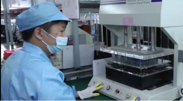
In-Circuit Testing
In-circuit testing (ICT) represents the most comprehensive type of PCB testing. This process, also referred to as a bed-of-nails test, involves the activation and powering up of individual components on the board.
Typically, the test aims for 100% coverage, although achieving coverage rates between 85-90%, free from human error, is more common. ICT is frequently employed for testing larger connections and ball grid arrays (BGAs).
This method is particularly suitable for “mature” products that are unlikely to undergo significant revisions.
Automated Optical Inspection
Automated Optical Inspection (AOI) employs either a single 2D camera or two 3D cameras to capture images of the PCB. The system then compares these images to a meticulously designed schematic. Any board that deviates from the schematic to a significant extent is marked for further inspection by a technician.
AOI can be beneficial for identifying issues promptly, thereby ensuring that production is halted promptly to prevent the dissemination of faulty products. However, it does not involve powering up the board and might not provide 100% coverage for all types of components.
Functional Testing
Certain customers prefer a traditional functional test to ensure their product’s functionality. This method to validate that the product can power up successfully. However this test necessitates specific requirements:
- External testing equipment
- Customized fixtures
- Compliance with industry standards such as UL, MSHA, and others.
The parameters and specifications for this functional test are typically provided by the customer. Kejie Circuits can assist in the development and design of such test. However, this testing method can be time-consuming, which may not be ideal for customers aiming to expedite product delivery.
From a quality and longevity perspective, functional testing can mitigate potential issues and reduce long-term costs.
Other Functional Testings
A PCB functional test validates the board’s performance within the intended product environment. The criteria, development, and execution of these tests can differ significantly based on the PCB and its final application.
Additional PCB assembly testing options include:
- Solderability test: Enhances the reliability of solder joints by ensuring a robust surface finish.
- PCB contamination testing: Identifies contaminants that could lead to corrosion or other issues.
- Micro-sectioning analysis: Examines defects, opens, shorts, and other failures.
- Time-domain reflectometer (TDR): Detects failures in high-frequency boards.
- Peel test: Assesses the strength required to separate the laminate from the board.
- Solder float test: Evaluates the thermal stress resistance of the PCB’s holes.
Flying Probe Testing
Flying probe testing serves as a cost-effective alternative to in-circuit testing. This non-powered testing method verifies the following: Opens, Shorts, Resistance, Capacitance, Inductance, Diode functionality.
The process involves the use of needles connected to a probe on an x-y grid, which is derived from the basic CAD design. The ECM program coordinates to align the circuit board with the test fixture and then executes the program. In certain cases, the need for flying probe testing can be obviated by in-circuit testing, provided the PCB is designed to accommodate the test fixture, thereby incurring a higher initial cost.
Despite its lower initial cost, flying probe testing might not be the most economical choice for large orders. It is important to note that a PCB flying probe test does not involve powering up the board.
Burn-in Testing
As the name implies, burn-in testing is an intensive form of testing for PCBs, specifically designed to uncover early failures and determine load capacity. This rigorous process can potentially damage the components being tested.
Burn-in testing involves subjecting the electronics to a power supply at an increased temperature, typically at or near their maximum specified operating temperature. Electronic components are more prone to failure during the initial phase of their operational life, with failure rates stabilizing in the middle and then increasing as they approach the end of their life cycle. If a PCB with an infant mortality failure were to be integrated into critical systems such as military or medical equipment, it could lead to a serious failure with significant consequences. By triggering latent defects through burn-in testing, the number of potentially catastrophic failures is reduced, thereby enhancing the reliability of the electronics for the original equipment manufacturer (OEM).
However, this approach comes with a trade-off: a lower yield and potentially shorter product lifespan. The data gathered from this testing can also be instrumental in helping engineers identify the root causes of defects and make design modifications to enhance product reliability before it reaches the burn-in stage.
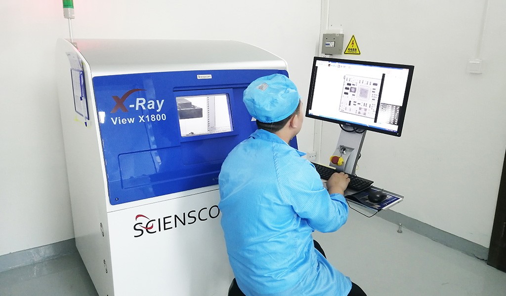
X-Ray Inspection
AXI, or Automated X-ray Inspection, serves as a non-destructive inspection tool for PCBs, offering both 2D and 3D imaging capabilities. The 3D variant typically provides faster inspection times.
X-ray inspection is particularly effective in examining components and solder joints that are not visible from the surface, such as those under ball grid array packages.
This method is highly beneficial but demands skilled and experienced operators for accurate analysis.
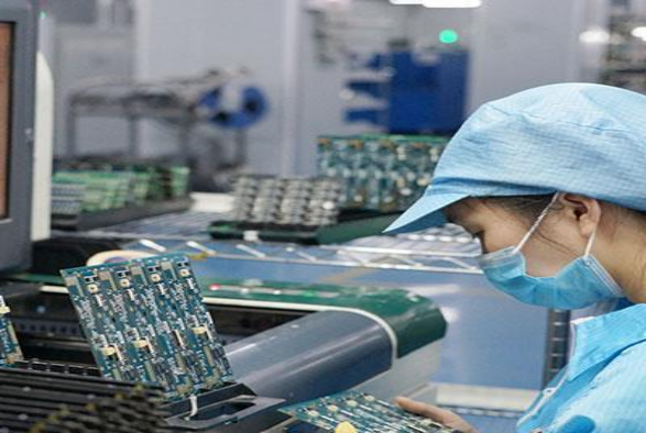
Visual Inspection
Manual visual inspection remains the most prevalent testing method, characterized by a minimal upfront cost, no need for test fixtures, and a single operator with a simple magnifying glass or microscope.
This method offers flexibility in adapting to product changes and is widely employed in major PCB manufacturing facilities. However, manual inspection is susceptible to operator subjectivity, necessitates significant training, and presents challenges in data collection and organization.
As PCB technology advances and customers demand higher reliability, mid to high-end PCB manufacturers are increasingly turning to automated equipment and instruments for inspection.
Kejie Pcb has been specializing in the manufacture and assembly of Printed Circuit Boards for over 25 years, with circuit board test qualifications and complete test programs. We will comprehensively determine the use of one or several test combinations for PCB testing according to the requirements of PCB design, use environment, and production cost.
- In-circuit testing (ICT)
- Automated optical inspection (AOI)
- Flying probe testing
- Burn-in testing
- Functional testing
- Other functional testing (solderability, contamination, and more)
- X-Ray inspection (AXI)
- Visual Inspection